
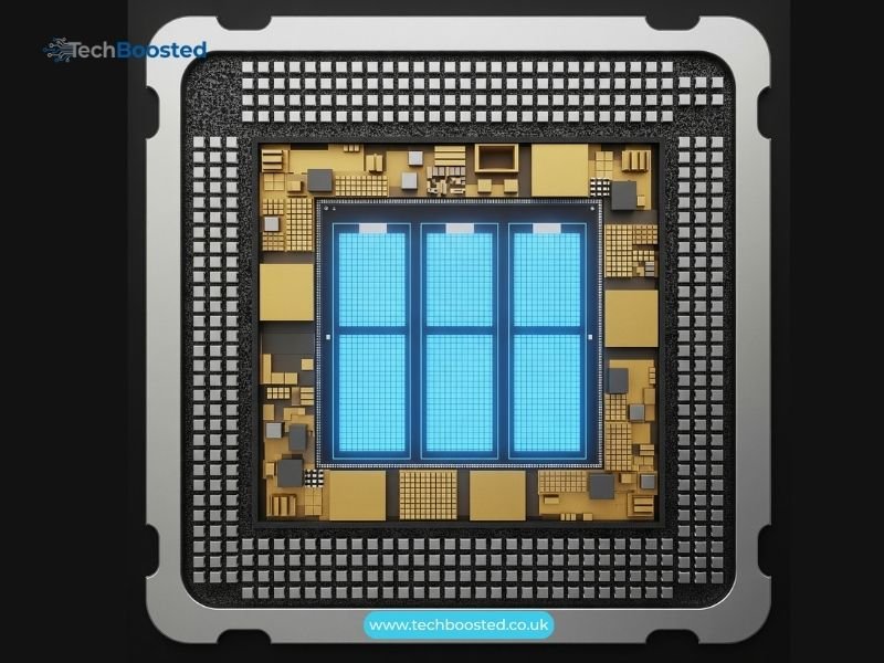
The Intel 18A process has emerged as one of the most significant advancements in semiconductor technology as of January 2026. It represents Intel’s first angstrom-era node and a true 1.8nm-class manufacturing process. This node combines cutting-edge transistor architecture with innovative power delivery solutions. Launched into high-volume production in late 2025, it officially debuted with the Intel Core Ultra Series 3 processors (Panther Lake) at CES 2026. The Intel 18A process incorporates RibbonFET gate-all-around transistors and PowerVia backside power delivery for the first time in commercial chips. These features deliver substantial improvements in performance per watt, transistor density, and overall chip efficiency. Production is ramping at Fab 52 in Arizona. Intel 18A powers next-generation AI-enabled laptops and servers.
Core Innovations Driving the Intel 18A Process
The Intel 18A process achieves its impressive capabilities through two groundbreaking technologies. These fundamentally change how chips are designed and powered. RibbonFET is Intel’s proprietary gate-all-around (GAA) transistor design. It replaces the FinFET structures used since the 22nm era. RibbonFET stacks multiple nanoribbons with the gate wrapped completely around each channel. This provides superior electrostatic control and dramatically reduces leakage current. The second-generation RibbonFET implementation includes refined ribbon widths. It also features dipole doping for precise threshold voltage tuning across eight levels. Enhanced drive current results in up to 15% better performance-per-watt compared to prior nodes. Paired with RibbonFET is PowerVia.
Advantages of RibbonFET Transistor Architecture
RibbonFET in the Intel 18A process enables unprecedented control over transistor behavior. Engineers can optimize for both high-performance and low-power scenarios within the same die. By stacking nanoribbons and fully encasing them with the gate, Intel achieves tighter channel control. This surpasses competing nanosheet designs. It minimizes off-state leakage that plagues ultra-small nodes. The architecture supports finer voltage scaling. It allows higher drive currents without increasing footprint. This makes it ideal for densely packed AI accelerators and mobile processors where thermal limits are critical. Early silicon results from Panther Lake and Clearwater Forest demonstrate reliable operation. Intel reported successful power-on and functional validation months ahead of schedule. These achievements highlight the technology’s readiness for high-volume manufacturing.
PowerVia: Transforming Chip Efficiency
PowerVia represents a paradigm shift in the Intel 18A process. It is the first backside power delivery technology deployed at scale in commercial products. Traditional front-side power routing creates congestion as nodes shrink. This forces trade-offs between signal integrity and power distribution. PowerVia resolves this by decoupling the two layers. Power is routed through the wafer backside via buried rails and through-silicon vias. Measurable benefits include lower resistance for reduced voltage droop. Thermal dissipation improves. Front-side area frees up for denser interconnects. In practical terms, PowerVia contributes up to 4% ISO-power performance gains. It enables more aggressive frequency scaling. This is particularly valuable for AI workloads demanding sustained high throughput.
Panther Lake: First Consumer Chip on Intel 18A
The Intel 18A process makes its consumer debut with Panther Lake. This is the compute tile powering Intel Core Ultra Series 3 mobile processors. They launched on January 27, 2026. These chips feature up to 16 hybrid cores. They include next-generation Xe3 integrated graphics and a powerful NPU for on-device AI. Generational leaps are substantial: up to 60% better multithreaded performance and 77% faster gaming compared to Lunar Lake predecessors. Fabricated entirely in the United States, Panther Lake showcases the node’s maturity. It handles complex, high-volume consumer products effectively. Intel’s disaggregated design approach shines here. Different tiles use optimized processes for cost efficiency.
Clearwater Forest: Data Center Dominance
For server applications, the Intel 18A process enables Clearwater Forest. Branded as Xeon 6+, it is scheduled for release in the first half of 2026. This all-E-core processor scales to an impressive 288 cores. It offers a 17% instructions-per-cycle uplift. Extreme density and power efficiency prioritize cloud and edge computing. Leveraging 18A’s density advantages and PowerVia’s thermal benefits reduces power consumption per workload. This attracts hyperscale operators focused on total cost of ownership. Multi-tile Foveros packaging demonstrates the node’s flexibility for large-scale designs.
Competitive Positioning Against TSMC N2
Compared to TSMC’s upcoming 2nm (N2) node, the Intel 18A process holds distinct advantages. These include power delivery and production timing. TSMC’s nanosheet transistors may achieve slightly higher density. Estimates are around 313 million transistors per square millimeter versus Intel’s 238 MTr/mm². However, Intel’s early backside power adoption provides superior efficiency in real-world scenarios, especially for AI and HPC workloads. Intel began risk production earlier. It entered high-volume manufacturing months ahead. This gives a lead in commercial deployment. Independent analyses suggest 18A outperforms in performance-per-watt metrics critical for modern computing.
Intel Foundry Growth and Major Customers
The success of the Intel 18A process accelerates Intel Foundry’s external business. Confirmed designs come from Microsoft for custom AI accelerators. Amazon Web Services uses it for data center silicon. These partnerships validate the node’s reliability and yield quality. Ongoing discussions with other hyperscalers signal growing diversification from single-source dependency. The U.S.-centric manufacturing footprint adds strategic value. It addresses global supply chain concerns. Intel positions as a resilient alternative for critical infrastructure.
Manufacturing Status and Yield Achievements
As of January 2026, the Intel 18A process operates in full high-volume production. The main site is Fab 52 in Arizona. Yields reportedly reach 60-65%. This is healthy for a new node and sufficient to support Panther Lake shipments. Capacity expands with additional tools coming online. Demand meets both internal products and foundry customers. Intel’s aggressive investment in domestic facilities ensures scalable output. Ongoing process optimizations target higher margins through 2026.
Future Extensions and Roadmap
The Intel 18A process serves as the foundation for enhanced variants. Examples include 18A-P for future refreshes with incremental improvements in density and power. Looking further ahead, it paves the way for the 14A node. This will incorporate high-NA EUV lithography. Intel maintains an aggressive cadence into the angstrom era. Sustained competitiveness in AI silicon leadership remains a key goal.
Conclusion
The Intel 18A process stands as a landmark achievement in semiconductor evolution. It successfully integrates RibbonFET and PowerVia technologies. Industry-leading efficiency and performance come in a domestically manufactured 1.8nm-class node. Proven products like Panther Lake and Clearwater Forest are already shipping. Strong foundry traction comes from Microsoft and Amazon. A clear production advantage exists over competitors. Intel has decisively reclaimed process technology leadership. As 2026 unfolds, 18A will drive transformative advancements. These span consumer AI PCs, data centers, and beyond. It reinforces the importance of resilient, innovative manufacturing for the future of computing.
FAQs
What makes Intel 18A different from previous nodes? It introduces RibbonFET gate-all-around transistors and PowerVia backside power delivery, the first commercial implementation of both technologies.
When did Intel 18A enter high-volume production? High-volume manufacturing began in late 2025, with first commercial products launching in January 2026.
Which processors use the Intel 18A process? Panther Lake (Core Ultra Series 3) for consumer laptops and Clear water Forest (Xeon 6+) for servers.
How does Intel 18A compare to TSMC’s 2nm? Intel leads in backside power delivery for better efficiency and started production earlier, while TSMC may have higher density.
Who are Intel Foundry’s customers for 18A? Confirmed customers include Microsoft for AI accelerators and Amazon Web Services for data center chips.
Where is the Intel 18A process manufactured? Primarily at Fab 52 in Arizona, United States, emphasizing domestic production.
For the latest CPU and semiconductor technology updates, stay connected with techboosted.co.uk on TechBoosted.co.uk!